The history of the PCB is relatively new, but as complicated and fascinating as the printed circuit boards themselves. Before the last half-century or so, few could have imagined how tiny traces on a printed circuit board, or PCB, connected with port headers and sockets, would fire up and function to make modern electronics possible. Before the PCB came along, each of those connecting traces required an intricate network of tangled wires to connect them. Building a TV or a computer required a complex mass of individual wires; and was a time-consuming, tedious undertaking.
Although the first circuit board patent design was in 1925 when American inventor, Charles Ducas, stenciled conductive materials onto a flat wooden board, it wasn’t until 1936 when Paul Eisler developed the first printed circuit board for use in a radio set. Eisler aided the American and British forces in the development of proximity fuses. These fuses, used by the military, were used in developing mines, bombs, and artillery shells during WWII. After the war, the U.S. Army released the PCB technology to the public. Eisler’s idea went to the next level; by embedding wires onto a flat piece of fiberglass, later used as a more advanced PCB design. The PCB was the new, exciting component that would make electronics less cumbersome and far easier to incorporate into the ever-growing world of technology.
History of the PCB
So, how exactly is the PCB designed, and how has it taken us from room-size board cabinets to carrying around our PCs? During the ’60s, an integrated circuit is born that puts thousands of components on a single chip. The IC improves the power, speed, and reliability of these devices. This technology led to an increase of conductors on the board, resulting in additional layers within the PCB. During this time, the IC chip becomes smaller; consequently, the PCB grows smaller; however, the soldering connections become less reliable. In the ’70s and ’80s, several advances come to the PCB. To reconcile the soldering complication, a thin lacquer-like layer polymer, called a soldermask, is developed for application to the copper traces of the printed circuit board. The solder mask protects against oxidation and prevents bridging between solder pads placed closely together. Denser boards with improved circuitry make way for new technology.
Surface mount technology, or SMT, is developed in the 1980s and quickly become the new industry standard. Previous technology required soldering each PCB component into PCB holes with wire leads. All the holes took up the space necessary for additional circuit routing. The SMT components could be soldered directly onto pads on the PCB, eliminating the need for holes; and opening prime real estate on the board. SMT technology not only improved the PCB performance, enhancing speed and reliability; it also made it more economical to produce. The ’90s see a decrease in size for the PCB and an increase in the use of manufacturing software.
Computer-aided design and manufacturing software helps automates design and aids in the elimination of several steps in PCB design. It encourages the use of a more elaborate, complex design, which can be carried out with tiny, lightweight components. This decade finds the components and connections growing smaller, more reliable, and increasingly inexpensive to manufacture. A multilayered, complex, flexible design is where the PCB finds itself in the 2000s. It has increased operational functionality and is seen in a multitude of electronic devices. Through the history of the PCB, they became progressively smaller and more efficient, lowering the cost, and increasing its span of use.
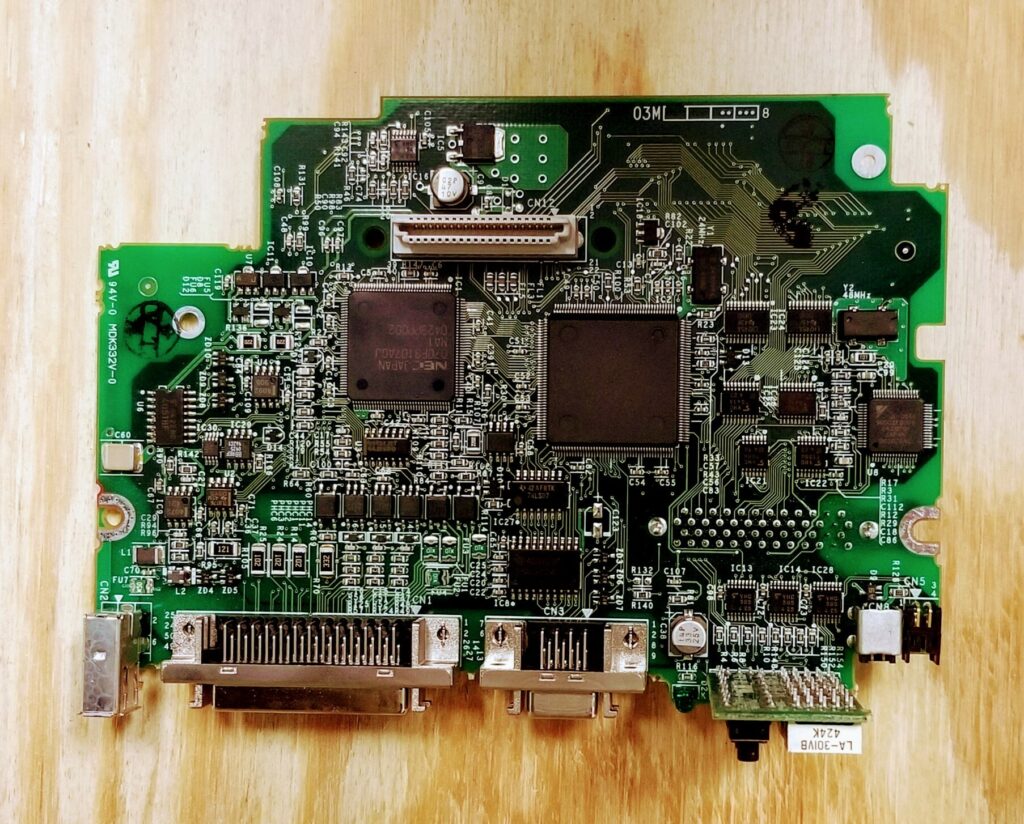
Making a PCB
The process of making the PCB board begins with resin-treated fiberglass, which is stacked together to create one sturdy piece. Copper, coated in a chemical called photoresist, is then applied to both sides of the fiberglass. The traces are placed on the top of the copper board in an exact pattern and exposed to UV light. The board is then washed, exposing the uncovered areas, leaving tracks of copper. These copper tracks are now our base that requires just a few more steps. The board will need etching a little more copper and a little more washing. This is a good place for a reminder that these steps are done in layers.
It is never a good idea to try to drill through a motherboard if you are experiencing mounting trouble. It may seem from the outside that you are avoiding the traces on the board, but you may inadvertently drill right through a trace within the layers of the board, rendering your board useless. Leave the drilling to the manufacturing factory. Holes are drilled through the PCB units at the factory for specified form factors and several other reasons. Accommodations are made in the PCB board for small electrical components such as resistors, chips, capacitors. Tiny interconnects between the different layers of copper traces are also drilled on the board. Now your board is ready for assembling additional components.
Once you mount or solder your components like your PCI Express slot, heat sink, or CPU sockets to the board, the board is essentially completed. To make a simple CPU board you do not need any lavish manufacturing processes since the PCU is just an assemblage of electrical connections on sort of a substrate.
PCBs Today and Beyond
What are the latest innovations in PCB technology? Today we have the ultra-light, ultra-thin rigid-flex printed circuit board. The rigid-flex PCB is a hybrid integrating aspects of both hardboard and flexible circuits. The benefit is a board that can be folded or flexed while maintaining the shape where necessary, offering the best in circuit design. With several looming advances in technology, who knows where the future of the PCB will land? If it is anything like the history of the PCB, the future of the PCB will be minute and impressive.
Updated on August 6, 2021 by Joe Kaminski